Metamorphic Epitaxial Materials:
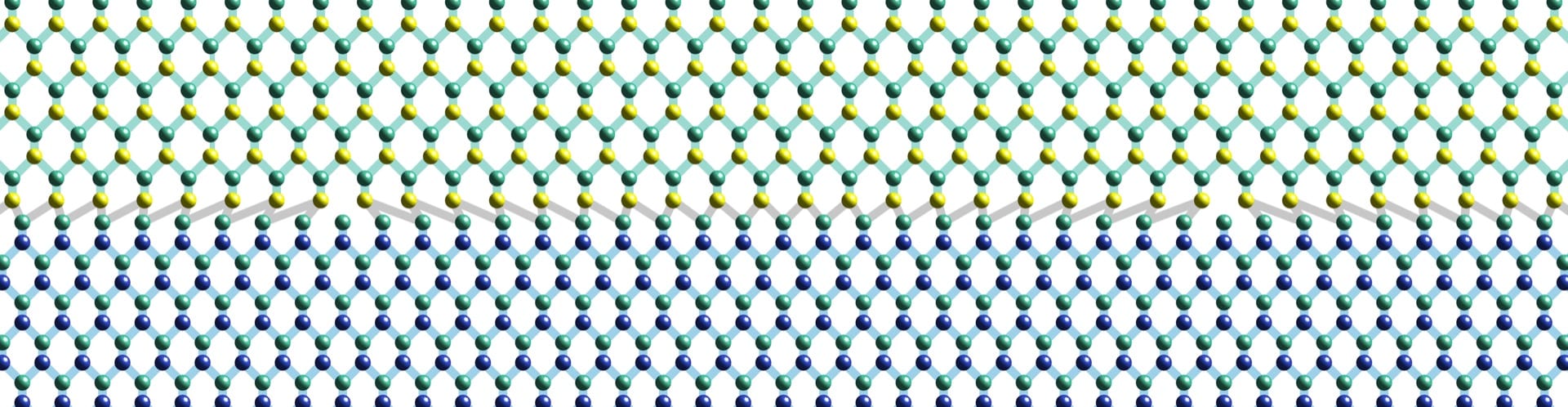
Atomic model of abrupt metamorphic interface between to III-V compound semiconductors with different lattice constants
Substrate selection for semiconductor lasers is conventionally dictated by satisfying near lattice matching of the desired gain material. We have shown that other engineering properties, such as thermal conductivity, can be used instead through the use of a metamorphic epitaxial materials. This project demonstrated that GaSb lasers can be grown metamorphically on GaAs substrate that outperform identical lasers grown pseudomorphically on GaSb substrates. The challenge of accomplishing this technological demonstration is the creation of a semicoherent interface between the GaSb epilayer and the GaAs substrate that exhibit a misfit strain of 6.7%. This misfit strain is accommodated within a few monolayers of the interface through a 2-dimensional array of misfit dislocations.
- C. J. K. Richardson and M. L. Lee, “Metamorphic epitaxial materials,” MRS Bulletin41, 193 (2016).
- C. J. K. Richardson, L. He, P. Apiratikul, N. P. Siwak, R. P. Leavitt, “Improved GaSb-based quantum well laser performance through metamorphic growth on GaAs substrates,” Applied Physics Letters 106, 101108 (2015).
- P. Apiratikul, L. He, R. P. Leavitt, N. P. Siwak, J. Duperre, C. J. K. Richardson, “2-micron GaSb-based metamorphic laser grown on GaAs,” Proceedings of SPIE 9002, 900216 (2014).
- L. He, L. E. Clinger, C. J.K. Richardson, “Stability of arsenide and antinomic surfaces during molecular beam epitaxy growth,” Journal ofVacuum Science and Technology B 32, 061204 (2013).
- P. Apiratikul, L. He, C. J. K. Richardson, “2-μm laterally coupled distributed-feedback GaSb-based metamorphic laser grown on a GaAs substrate,” Applied Physics Letters 102, 231101 (2013).
- C. J. K. Richardson, L. He, S. Kanakaraju, “Metamorphic growth of III-V semiconductor bicrystals,” Journal of Vacuum Science and Technology B 29, 03C126 (2011).
AlGaAs Nanowire Nonlinear Waveguides
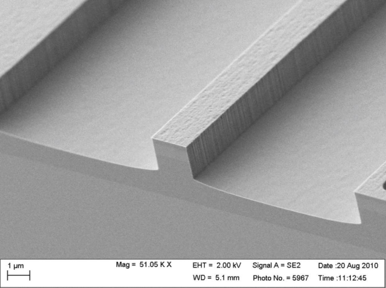
Sub-micron wide AlGaAs nonlinear waveguide
Optically nonlinear nanowire waveguide performance is dictated by material nonlinearity combined with waveguide loss and dispersion. Through this project we achieved optimization of the waveguide materials by minimizing material loss and two-photon absorption. We also advanced waveguide fabrication techniques to create smooth sidewall sub-micron waveguides with record low scattering loss. These devices were used to demonstrate record four-wave mixing efficiency and bandwidth, and used in the first demonstration of a semiconductor nonlinear waveguide to perform optical data format conversion of phase-encoded signals.
Select publications related to AlGaAs nanowire nonlinear waveguides:
- T. Mahmood, W. Astar, B. Cannon, P. Apiratikul, G. A. Porkolab, C. J. K. Richardson, G. M. Carter, “Polarization-Insensitive Wavelength Conversion by FWM of 100-GHz-Spaced DWDM 4 x 10 Gb/s RZ-BPSK Signals in a Birefringent Nonlinear AlGaAs Waveguide,” IEEE Journal of Quantum Electronics 5074 (2014).
- G. A. Porkolab, P. Apiratikul, S.-H. Guo, C. J. K. Richardson, “Reducing sidewall roughness of sub-micrometer-scale waveguides using nitrogen plasma-assisted reflow,” Optics Express 22, 7733 (2014).
- J. J. Wathen, P. Apiratikul, C. J. K. Richardson, G. A. Porkolab, G. M. Carter, T. E. Murphy, “Efficient continuous-wave four-wave mixing in bandgap-engineered AlGaAs waveguides,” Optics Letters 39, 3161 (2014).
- P. Apiratikul, J. J. Wathen, G. A. Porkolab, B. Wang, L. He, T. E. Murphy, C. J. K. Richardson, “Enhanced continuous-wave four-wave mixing efficiency in nonlinear AlGaAs waveguides,” Optics Express 22, 26814 (2014).
- B. M. Cannon, W. Astar, T. Mahmood, P. Apiratikul, G. A. Porkolab, C. J. K. Richardson, G. M. Carter, “Data transfer from RZ-OOK to RZ-BPSK by polarization-insensitive XPM in a passive birefringent nonlinear AlGaAs waveguide,” Journal of Lightwave Technology 31, 952 (2013).
- B. M. Cannon, W. Astar, T. Mahmood, P. Apiratikul, G. Porkolab, P. Bourda, T. Mohsenin, C. J. K. Richardson, G. M. Carter, “All-optical amplitude-phase transmultiplexing of RZ-OOK and RZ-BPSK to RZ-QPSK by polarization-insensitive XPM using a nonlinear birefringent AlGaAs waveguide,” Optics Express 21, 19885 (2013).
MBE Semiconductor Growth Science
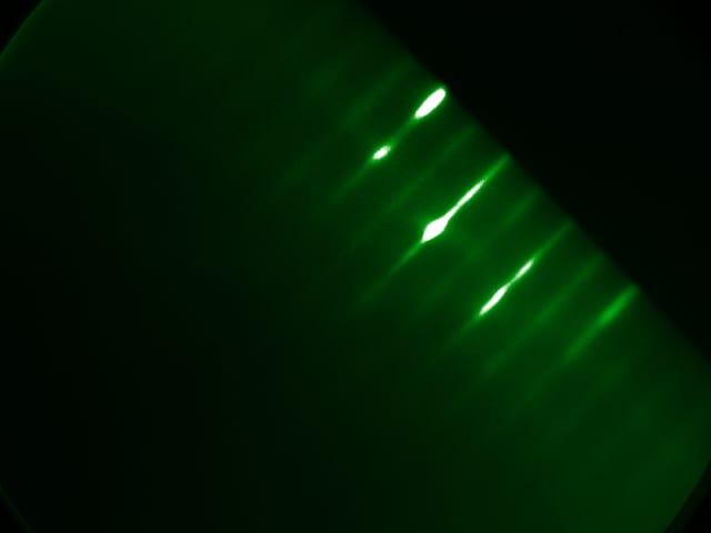
RHEED image of GaAs arsenic terminated surface
The study of fundamental growth science of compound and alloy superconductor materials. Studies include thermodynamic & kinetic investigations into growth, surfaces, and reactions. Advancement in materials characterization and prototype device evaluation.
Select publications related to MBE semiconductor growth science:
- L. He, L. E. Clinger, C. J.K. Richardson, “Stability of arsenide and antimonide surfaces during molecular beam epitaxy growth,” Journal ofVacuum Science and Technology B 32, 061204 (2013).
- D. Ali, C.J.K. Richardson, “Comparison of BeO and pyrolytic graphite crucibles for boron doped silicon epitaxy,” Journal of Vacuum Science and Technology A 30, 061405 (2012).
- J Hackley, W. L. Sarney, C. J. K. Richardson, “Antimony-assisted carbonization of Si(111) with solid source molecular beam epitaxy,”Journal of Vacuum Science and Technology A 31, 061511 (2013).
- R. P. Leavitt, L. He, C. J. K. Richardson, “Dual-superlattice calibrations for group-III species in III-V semiconductor epitaxial structure growth, “Journal of Vacuum Science and Technology B 32, 041205 (2014).
Optoelectronic Materials and Devices
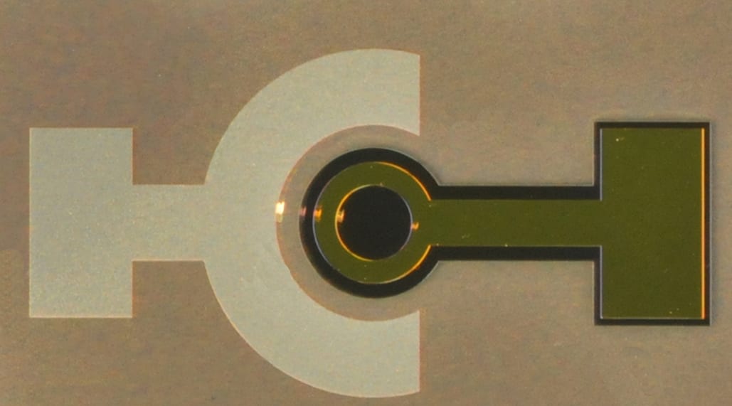
Mesa photodetector
Both self contained and collaborative research projects have developed a large array of devices for optical communications including lasers, semiconductor optical amplifiers, electroabsorption modulators, ring resonators, various types of photodetectors, MEMs and integrated devices.
Select publications related to optoelectronic materials and devices:
- C. J. K. Richardson, L. He, P. Apiratikul, N. P. Siwak, R. P. Leavitt, “Improved GaSb-based quantum well laser performance through metamorphic growth on GaAs substrates,” Applied Physics Letters 106, 101108 (2015).
- P. Apiratikul, L. He, C. J. K. Richardson, “2-μm laterally coupled distributed-feedback GaSb-based metamorphic laser grown on a GaAs substrate,” Applied Physics Letters 102, 231101 (2013).
- D. Ali, C. J. K. Richardson, “Strain-balanced Si/SiGe type-II superlattices for near-infrared photodetection,” Applied Physics Letters105, 031116 (2014).