Superconductors for Superconducting Quantum Circuits
Our superconductivity research targets materials for use in quantum information science. The key metric is microwave loss, not high Tc. With the philosophy of improving structure-property-performance relationships the role of epitaxial materials, atomic structure, and contamination have been explored in elemental and transition metal nitride superconductors such as Al, TiN, and NbN. Our goal of creating an epitaxial all-nitride Josephson junction and quasi-particle traps is extending this line of research from low loss linear circuit elements to future, low-loss nonlinear superconducting circuit elements
- C. J. K. Richardson, A. Alexander, C. G. Weddle, B. Arey, and M. Olszta, “Low-loss superconducting titanium nitride grown using plasma-assisted molecular beam epitaxy,” Journal of Applied Physics 127, 235302 (2020).
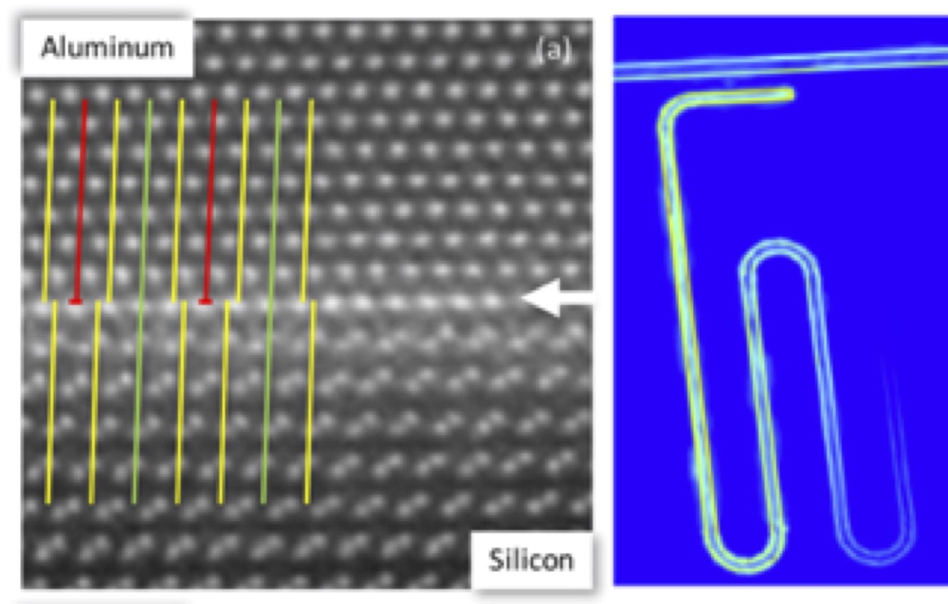
- X.-Y. Liu, B. Arey, I. Arslan, J. Hackley, V. Lordi, and C. J. K. Richardson, “Perfect strain relaxation in metamorphic epitaxial aluminum on silicon through primary and secondary interface misfit dislocation arrays,” ACS Nano 12, 6843 (2018).
- A. Alexander, B. M. McSkimming, B. Arey, I. Arslan, and C. J. K. Richardson, “Nucleation and Growth of Metamorphic Epitaxial Aluminum on Silicon (111) 7×7 and √3×√3 Surfaces,” Journal of Materials Research 322, 4067 (2017).
- B. M. McSkimming, A. Alexander, M. H. Samuels, B. Arey, I Arslan, and C. J. K. Richardson, “Metamorphic growth of relaxed single crystalline aluminum on silicon (111),” Journal of Vacuum Science and Technology A 35, 021401 (2017).
- C. J. K. Richardson, N. P. Siwak, J. Hackley, Z. K. Keane, J. E. Robinson, B. Arey, I. Arslan, B. S. Palmer, “Fabrication artifacts and parallel loss channels in metamorphic epitaxial aluminum superconducting resonators,” Superconductor Science and Technology 29, 064003 (2016).
- J. H. M. Iftekhar, J. A. Aguilar, B. Sarabi, Y. J. Rosen, A. N. Ramanayaka, E. H. Lock, C. J. K. Richardson, K. D. Osborn, “Superconducting TiN Films sputtered over a large range of substrate DC bias,” IEEE Transactions on Applied Superconductivity 25, 1100505 (2014).
Silicon Germanium Quantum Dot Material
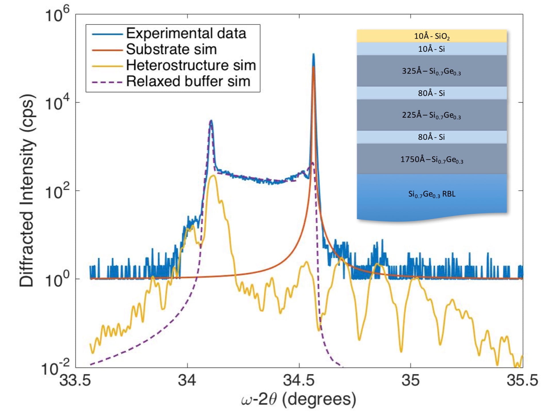
Our research in semiconductor materials focuses on the growth of metamorphic silicon germanium heterostructure in order to produced high quality strained-silicon or strained-germanium quantum wells. Our focus is on the characterization and growth of these engineered materials.
- C. J. K. Richardson, C. A. C. Jackson, L. F. Edge, and P. W. Deelman, “High-resolution x-ray reflection Fourier analysis of metamorphic Si/SiGe quantum wells,”Journal of Vacuum Science and Technology B 35, 02B113 (2017)
- D. Ali, C.J.K. Richardson, “Reflection high-energy electron diffraction evaluation of thermal deoxidation of chemically cleaned Si, SiGe, and Ge layers for solid-source molecular beam epitaxy,” Journal of Vacuum Science and Technology A 30, 061405 (2012).
Quantum Dot Quantum Emitters
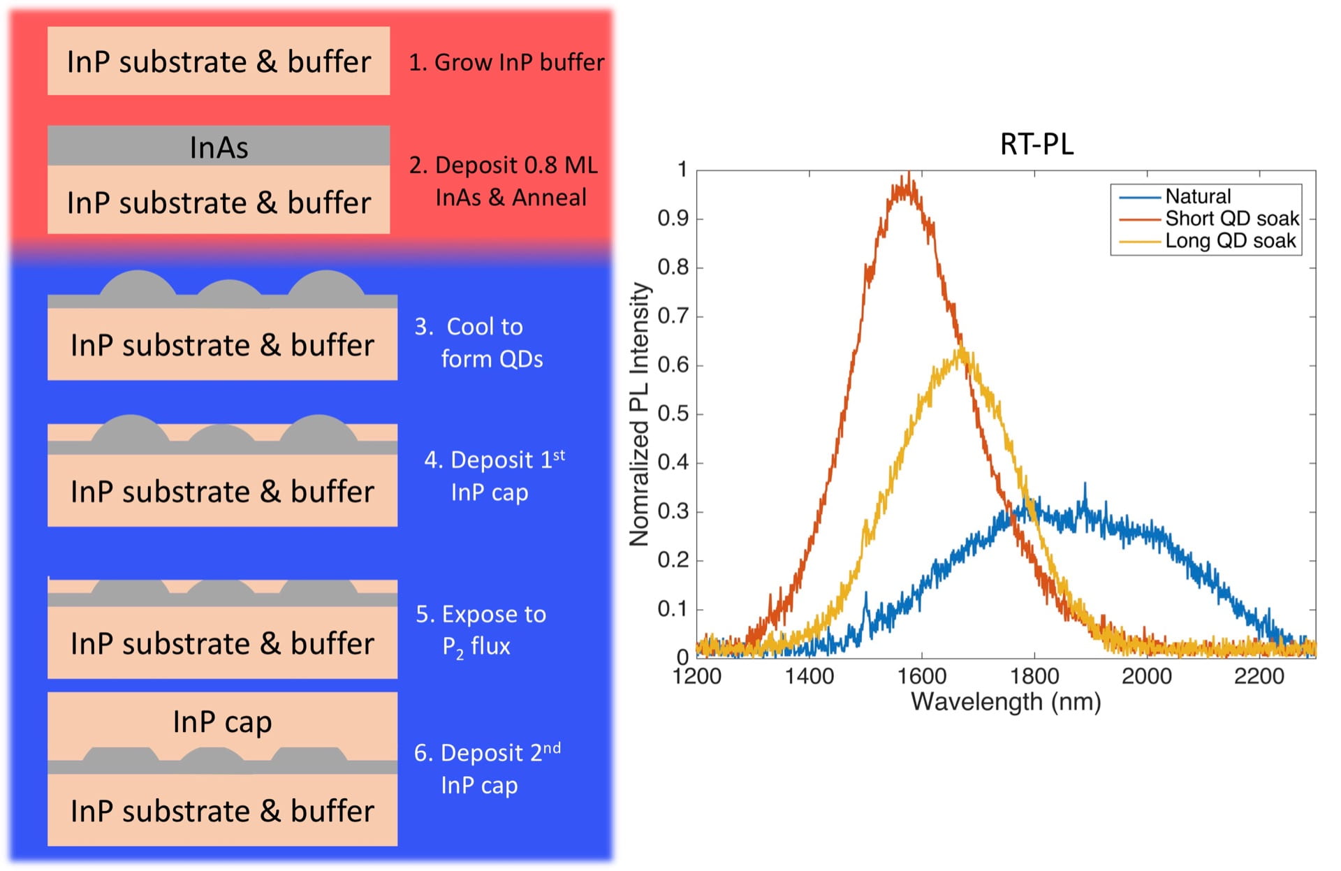
We developed a modified-Stranski Krastanov growth technique to synthesize circular InAs quantum dots on InP surfaces that have a controllable density and emission out to 1400 nm. Long-distance quantum communication relies on the ability to efficiently generate and prepare single photons at telecom wavelengths. Our collaborators have published multiple demonstrations of the indistinguishable photons created by incorporating these quantum dots into various photonic cavities.
- C. J. K. Richardson, R. P. Leavitt, J.-H. Kim, E. Waks, I. Arslan, and B. Arey, “Origin of Spectral Brightness Variations in InAs/InP Quantum Dot Telecom Single Photon Emitters, “Journal of Vacuum Science and Technology B PAULH2019, 011202 (2019).
- J.-H. Kim, S. Aghaeimeibodi, C. J. K. Richardson, R. P. Leavitt, and E. Waks, “Super-radiant emission from quantum dots in a nanophotonic waveguide,” Nano Letters 18, 4734 (2018).
- J.-H. Kim, S. Aghaeimeibodi, C. J. K. Richardson, R. P. Leavitt, D. Englund, and E. Waks, “Hybrid Integration of Solid-State Quantum Emitters on a Silicon Photonic Chip,” Nano Letters 17, 7394 (2017).
- J.-H. Kim, C. J. K. Richardson, R. P. Leavitt, and E. Waks, “Two-Photon Interference from the Far-Field Emission of Chip-Integrated Cavity-Coupled Emitters,” Nano Letters DOI: 10.1021/acs.nanolett, 6b03295 (2016).
- J.-H. Kim, T. Cai, C. J. K. Richardson, R. P Leavitt, E. Waks, “Two-photon interference from a bright single-photon source at telecom wavelengths,” Optica 3, 577 (2016).
- R. P. Leavitt and C. J. K. Richardson, “Pathway to achieving circular InAs quantum dots directly on (100) InP and to tuning their emission wavelengths toward 1.55 μm,” Journal of Vacuum Science and Technology B 33, 051202 (2015).